

Professional Instrument Distribution
Precision Inspection
Empowering Smart Manufacturing
Professional distributor of precision inspection instruments including microscopes, scanning electron microscopes (SEM), 3D optical profilers, and CT systems. We provide full-lifecycle technical services for universities, research institutes, electronics & semiconductor industries, and advanced manufacturing sectors.
10+
Years of Industry Experience
500+
Serve customers
9
Major Product Categories
Brands
Agent Brand
Authorized distributor for leading domestic and international precision instrument brands, ensuring authentic products and original manufacturer technical support.




Core Products
Distributor of leading international brands, delivering complete instrument solutions for everything from microscopic observation to precision measurement.
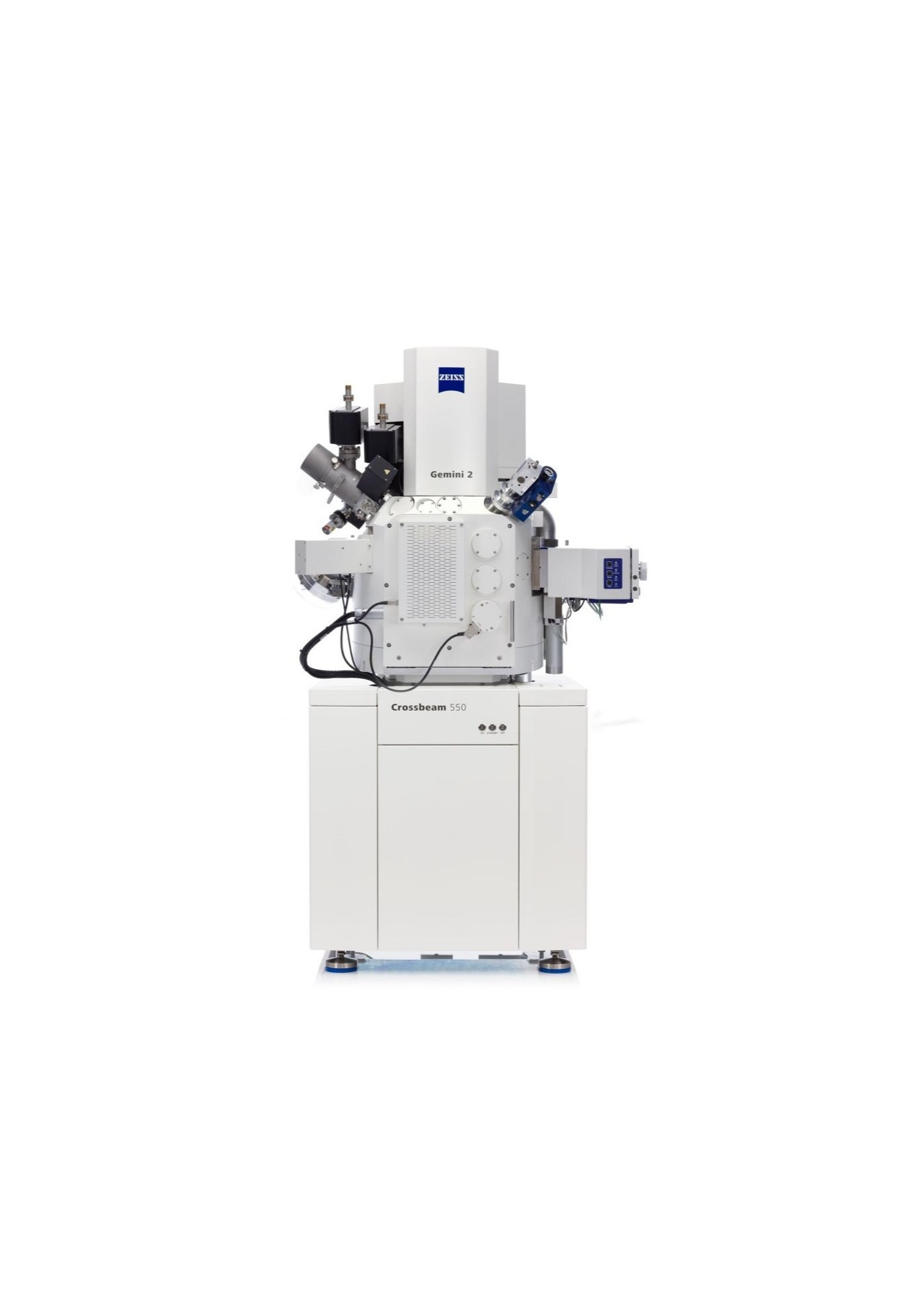
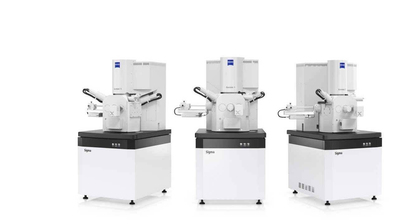
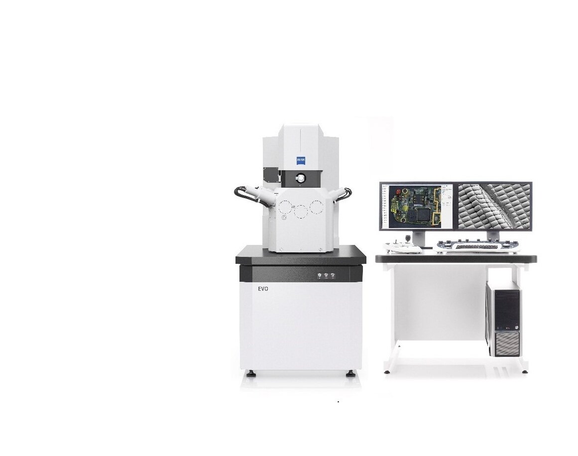
Scanning Electron Microscope
Covers the full range of optical microscopes, including upright, inverted, and stereo models, for applications in materials science, life sciences, and more.
View details›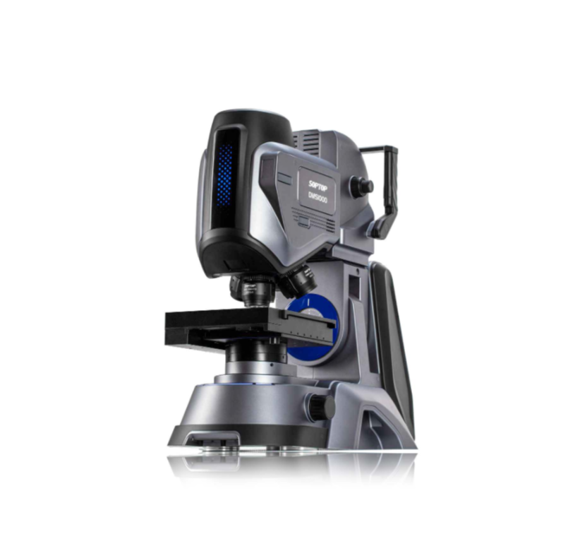
Optical Microscope
High-Resolution Surface Topography Analyzer with Nanoscale Imaging and Elemental Analysis
View details›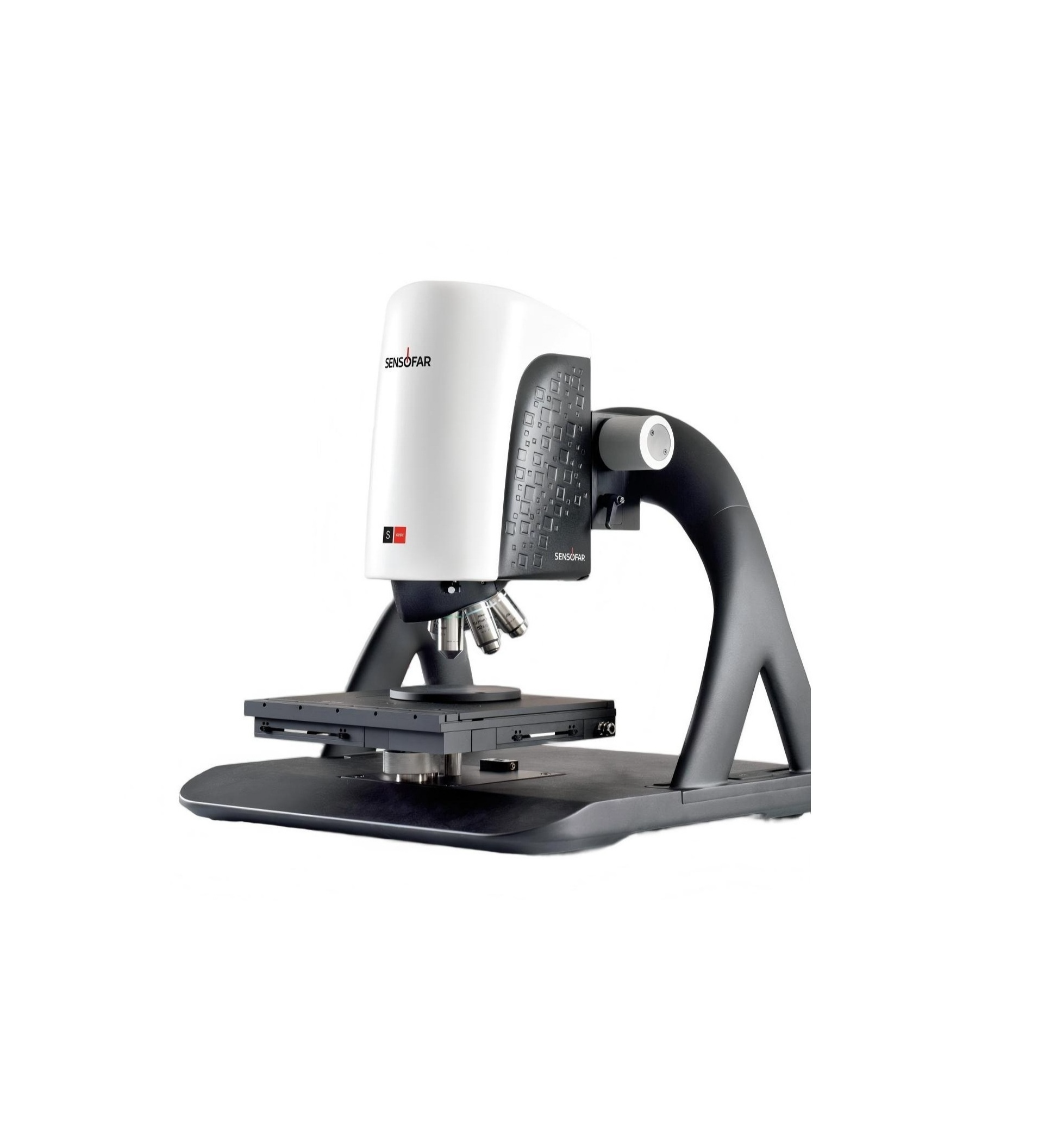
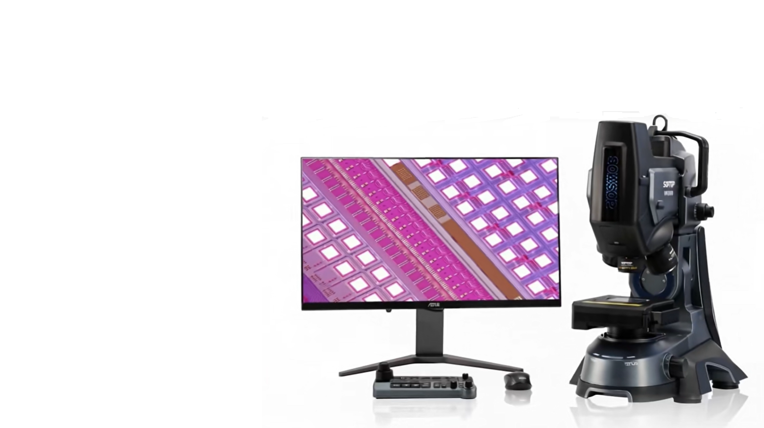
3D Optical Profiler
Non-contact 3D surface profilometer for sub-nanometer precision measurement
View details›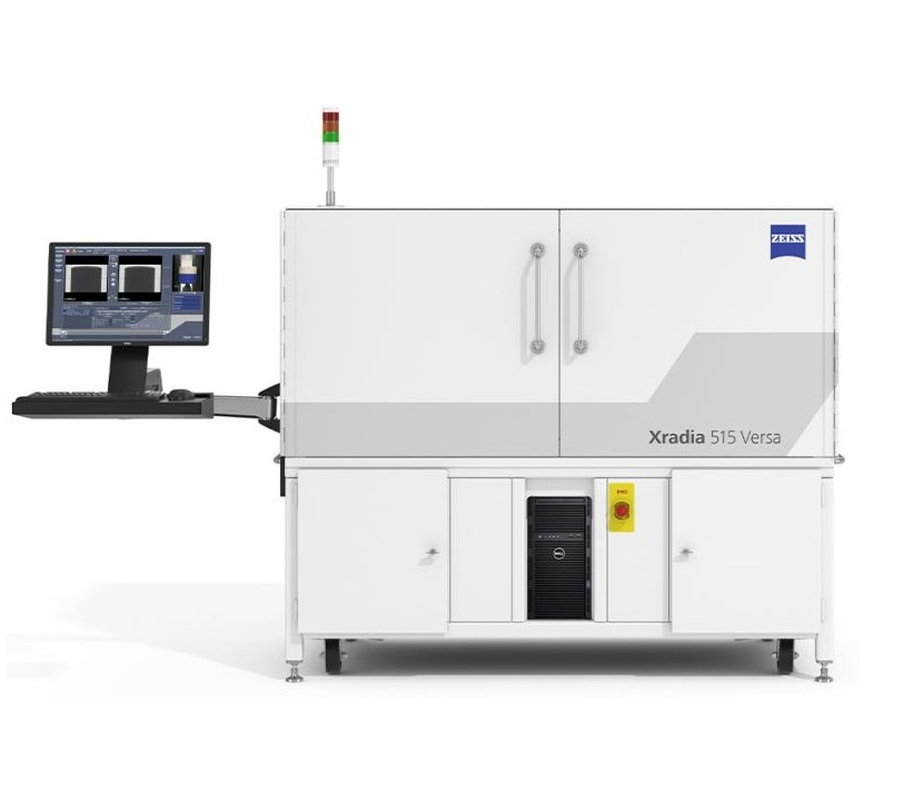
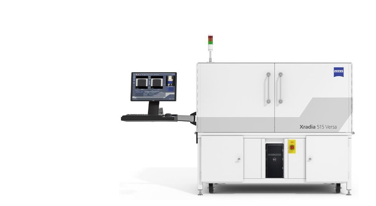
CT Inspection System
Industrial CT System for Non-Destructive Internal Inspection and 3D Reconstruction
View details›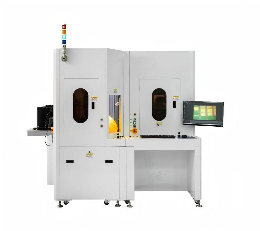
Wafer Inspection System
The wafer inspection system combines stability and safety to reliably transport wafers, making it ideal for inspections across front-end to back-end processes. Available in three models—AWL046, AWL068, and AWL812—it supports wafer sizes from 4 to 12 inches, offering broad applicability and flexible configurations. Its freely configurable inspection modes are designed with ergonomics in mind, ensuring comfortable and intuitive operation.
View details›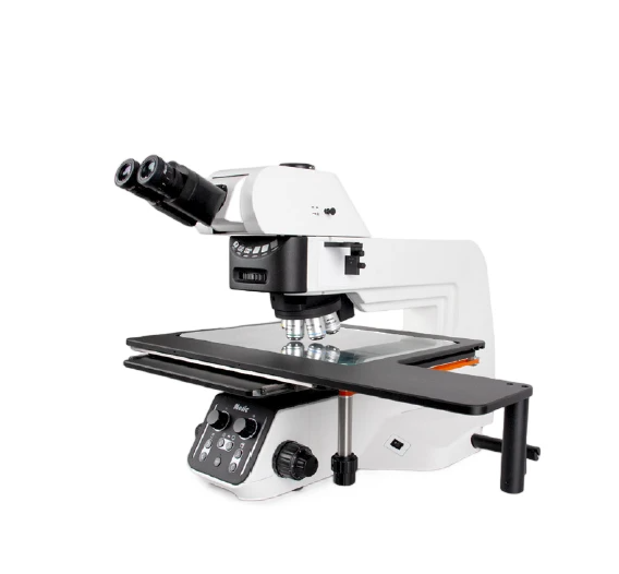
Precision Optical Measuring Instrument
Covers the full range of optical microscopes, including upright, inverted, and stereo models, for applications in electronics, semiconductors, materials science, and life sciences.
View details›App Center
Covering cutting-edge fields such as semiconductors, materials science, life sciences, and precision manufacturing with professional instrumentation solutions.

Zhitongfang showcases at the 2024 China International Scientific Instrument Exhibition
Our company will showcase a range of new precision instruments, presenting the latest solutions for microscopic analysis and non-destructive testing.

Trends in Semiconductor Inspection Technology: From Microns to Nanometers
Exploring the Evolution of Precision Inspection Equipment in Advanced Process Nodes

Application of Scanning Electron Microscopy in Lithium Battery Material Research
Analyze cathode material microstructure and interfacial structure using field-emission SEM

Daily Maintenance and Care Guide for Metallographic Microscopes
Key Maintenance Tips and Troubleshooting for Extending Device Lifespan
Benefits
Why Choose Zhitong Tongfang
Partner with us for expert technical capabilities and a comprehensive service system.
100%
Authentic Authorized
All products are sourced directly from authorized brand channels, complete with full traceability documentation and warranty coverage.
50+
Professional Technical Team
The application engineering team has an average of over 8 years of experience, providing in-depth technical support.
24h
Quick Response
Technical support response within 24 business hours; priority handling for urgent issues.
full lifecycle
Full Lifecycle Services
From selection consulting, installation and debugging, training guidance to regular maintenance—we're with you every step of the way.
News & Insights
Stay updated with Zhihe Tongfang's latest news and industry insights
Zhite Tongfang to Showcase at 2024 China International Scientific Instrument Exhibition
Our company will showcase a range of new precision instruments at the exhibition, featuring the latest solutions for microscopic analysis and non-destructive testing.
Read more›Trends in Semiconductor Inspection Technology: From Micron to Nanometer Scale
Exploring the Evolution of Precision Inspection Equipment for Advanced Process Nodes
Read more›Applications of Scanning Electron Microscopy in Lithium Battery Material Research
Analyze the microstructure and interface of cathode materials using field-emission SEM.
Read more›Contact Us
Leave your contact information, and our expert team will provide you with a customized solution.
Company Address
Room 315, Tsinghua University High-End Research Institute, Building 4, Huaminc Valley Science and Technology Innovation Park, Huaiming High-tech Zone, Dongli District, Tianjin
Contact Number
18722100128
leeyangok@sina.cn
Working Hours
Monday to Friday 9:00-18:00
Company Location
Room 315, Tsinghua University High-End Research Institute, Innovation Valley of Huiming High-Tech Zone, Dongli District, Tianjin, Building 4

